Chip Design
The world sees a chip – we fabricate its flawless anatomy
Innovative Semiconductor Design
Simplifying design complexities while accelerating GTMs
Analog to digital to mixed signal VLSI chips are getting more complex daily. Accordingly, expectations across semiconductor companies are shifting. Teams are required to innovate, constantly pushing the limits of semiconductor design, and companies need end-to-end VLSI design competence in one partner to maintain operational cost control and accelerate release.
From ideation to design innovation and validation – we offer chip solutions for seamless and superior ASIC design, powering next-gen product realization for manufacturers.
Design Engineering At A Glance
Focus on first-time-right VLSI design with robust infrastructure
As the VLSI engineering partner of manufacturers & semiconductor companies, we continuously hone our ASIC design capabilities. Our experts bring efficiency into every step with robust infrared support, from concept to flawless VLSI chip specifications to faster tape-outs.
The outcome – better VLSI design architecture and best-in-class testing ensure a first-time-right turnkey solution.
From The Experts’ Eye
The next in our VLSI design and its growth story
Experience how we etch market leadership on VLSI growth strategy through horizontal skill development and vertical solutions.
Detailing Chip Design Capability
DFT to error-free physical design – precision end-to-end
Analog & Mixed Signal (AMS) Design
Command over and AMS design and layout
The Analog and Mixed-signal design team at Tessolve specializes in high-quality custom chip design for applications with process nodes varying from 350 nm to most advanced 3nm designs. The IPs were developed for various industry verticals like Automotive, Communication, Consumer, Medical, IoT, etc. The competent team has rich experience in delivering chip solutions of more than 70+ silicon-proven Analog chips during the last few years with full ownership of the delivery from Spec to GDSII signoff, supported with silicon validation to global semiconductor companies.
Highlights
- Complete Analog Design life cycle from specs to post-silicon validation.
- Expertise in developing Full IP & Block level
- Offers in CMOS/FinFET process nodes: 3nm, 5nm, 7nm, 10nm, 14nm, 22nm, 45nm, 65nm, 90nm, 130nm, 180nm & 350nm
RTL Design
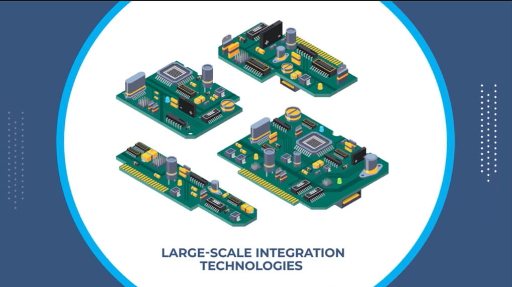
Large-scale RTL integration competence
Tessolve offers RTL design services from product specifications for both IP and SOC Development. Offerings include:
Tessolve offers RTL design services from product specifications for both IP and SOC Development. Offerings include:
Highlights
- Standard and Complex IP Block Design and Development
- SoC and Subsystem Integration, Clock and Reset design, Clock gating, Low-power chip design, UPF definition
- RTL Quality Checks: Lint, CDC, Automated property checks, Low-power checks
- Protocol Experience: HSIO Protocols (PCIe, USB, MIPI), AMBA protocols (AXI/AHB/APB), Memory interfaces (DDRx/LPDDRx), Low-speed peripheral interfaces (I2C, SPI, UART, MDIO, I2S)
Design Verification
Sector-agnostic verification expertise
Verification is one of the most significant tasks in silicon development and has the most significant impact on the critical business drivers of quality, schedule, and cost. Tessolve, a chip design solution, has a large pool of verification resources and investments in tools and verification methodologies, helping semiconductor companies fulfill their validation needs.
Highlights
- IP and SOC-level Verification using C/C++, SV-UVM methodologies
- CPU (ARM, RISC-V, Tensilica) processed based on verification
- Robust Verification planning to achieve Functional and Code Coverage goals
- Power-aware verification
- Gate-level simulations and regression management
- Tools for verification productivity – Formal Verification, PSS
Design for Test (DFT)
Demystifying design for test and debugging
Our Design for Testability experts team can help with the chip DFT architecture and implementation to increase IC test coverage, yields, and quality. Coupled with our large ATE test team and infrastructure, we are uniquely placed to build a coherent strategy and implement DFT that improves the testability of the IC in the post-silicon phase for first-pass silicon. Tessolve’s DFT service offerings include the following:
Highlights
- DFT architecture and scan methodology
- RTL-level DFT quality checks
- Scan insertion, ATPG pattern generation, and verification
- Memory BIST and Boundary Scan
- Fault Coverage Analysis, Debug, and Improvement
- Post-silicon debug support
DFT
Implementing DFT for a network SoC
Case Study PDF Download
End-to-end DFT for a consumer SoC
Case Study PDF Download
Physical Design
Expertly outlining physical layers in chip anatomy
Physical design is a process in VLSI engineering in which the structural netlist is transferred from the front-end design to the back-end design team to transform into a physical layout database containing geometrical design information for every physical layer and is used for interconnections. Tessolve’s physical implementation services include:
Motivated team, better design capability
Rich and extensive experience in physical design (PD) has enabled the team to work on multiple successful tape-outs. Expertise with all Industry standard EDA tools and design Flow, and well-trained to handle low power, high-performance area critical designs.
Highlights
- Executed multiple Mixed Signal SOCs from spec to silicon in parallel.
- Specialized in complex IP’s and subsystems in Graphics, Processors, PCIE-Gen5, CXL3.0, GDDR6, LPDDR4, and Automotive domains.
- The timing closure of high-frequency designs is up to 3Ghz, and technology is down to 3nm.
- Development of complex Low Power SPEC & Implementation
- Development of Timing, Sign Specs, and comprehensive checklists.
FPGA and Emulation
Complex design samples – tested and validated
Experience emulating and prototyping complicated IC designs for quick system debugging and software bring-up.
Prototyping across multi-platforms – we make it possible
The team has extensive experience executing FPGA programs for customers across the Networking, Automotive, Industrial, and Consumer Electronics domains. The team has delivered 80 + FPGA products with multiple specs involving the bit-file generation and validation programs. Expertise areas include high-speed Interconnects, Bus Interfaces, Network Protocols, SoC Interfaces, Audio/Video Applications, and Controllers.
We offer a full-service spectrum covering FPGA Design, FPGA Prototyping, and Emulation Flows.
Highlights
- Experience with the AMD & Intel FPGA device family
- FPGA-based emulation, FPGA partitioning, ASIC to FPGA & FPGA to ASIC conversion
- Custom board development and FPGA validation
Spotlight On Team Expertise
- Extensive experience in successfully executing FPGA programs for customers across Networking, Automotive, Industrial, and Consumer Electronics domains.
- Has delivered 80 + FPGA products with multiple specs involving the bit-file generation and validation programs.
- Expertise areas include high-speed Interconnects, Bus Interfaces, Network Protocols, SoC Interfaces, Audio/Video Applications, and Controllers.
Foundry Porting Services
Mapping our excellence in realizing foundry shifts
The fundamental aim of the foundry porting service is to take an existing VLSI design and retarget it to a new technology/foundry while retaining the exact functionality and specs of the original design.
- Translating parameters is complex while moving to a new foundry.
- There might be differences between size and parameters while using the new foundry.
Diving Into The Analog Porting Process
- Transferring and adapting the schematic, layout, and test benches from the source to the target foundry.
- Involves using automation flows as much as possible for a quick turnaround time while reducing the manual porting effort.
- Building any required portable test benches for analog porting and a source and target foundries verification environment.
- For migrating schematic, scripts should handle physical differences in symbols and then deal with parameter names and values.
- Any required scripts are created during this process to migrate the schematic between source and target technologies.
- These scripts can be easily reused for the same pair of source and target technologies for different designs.
- The schematic and the test benches are connected to the new model files, and the design is ready for simulation.
- A full suite of verification will be carried out on the migrated design.
The Steps We Follow In Our Approach

Requires the schematic view of the design to be followed for the new foundry process. We run the migration script from the source to the destination database to get the schematic view.

Verifying the device mapping for all blocks in the destination process technology. If it’s good, we will simulate selected blocks in source and destination model libraries and generate a comparison table. Results point to the blocks to be replaced for the new foundry design.

Suppose the comparison between source and destination simulation is okay. In that case, we run the migration script on the source-to-destination database for layout views with necessary/required manual tweaks and run the verification flows.

If the comparison is not okay, then proceed to manual porting techniques. Then, run the DC simulation on the source technology, find out the operating points of all the transistors, and replicate it in destination technology.

Post simulations comparison view and check if the specifications are ok. If it is okay, we will tweak the design to replicate the source technology characteristics and generate a comparison view. If the comparison view is ok, run the migration script from the source to the destination database.

Generate the post-layout netlist and compare it with the pre-layout simulation if the layout is verified and accepted by the requirements of the company.

Avail VLSI Design Expertise
The demand for innovation is pushing companies to explore new frontiers, challenging the limits of semiconductor design. Tessolve is a leading VLSI design provider. We help companies with our end-to-end VLSI engineering design services. At Tessolve, we offer solutions for various designs, such as AMD design, RTL design, DFT & physical design, and testing. Leverage unparalleled VLSI design in the USA with Tessolve.


