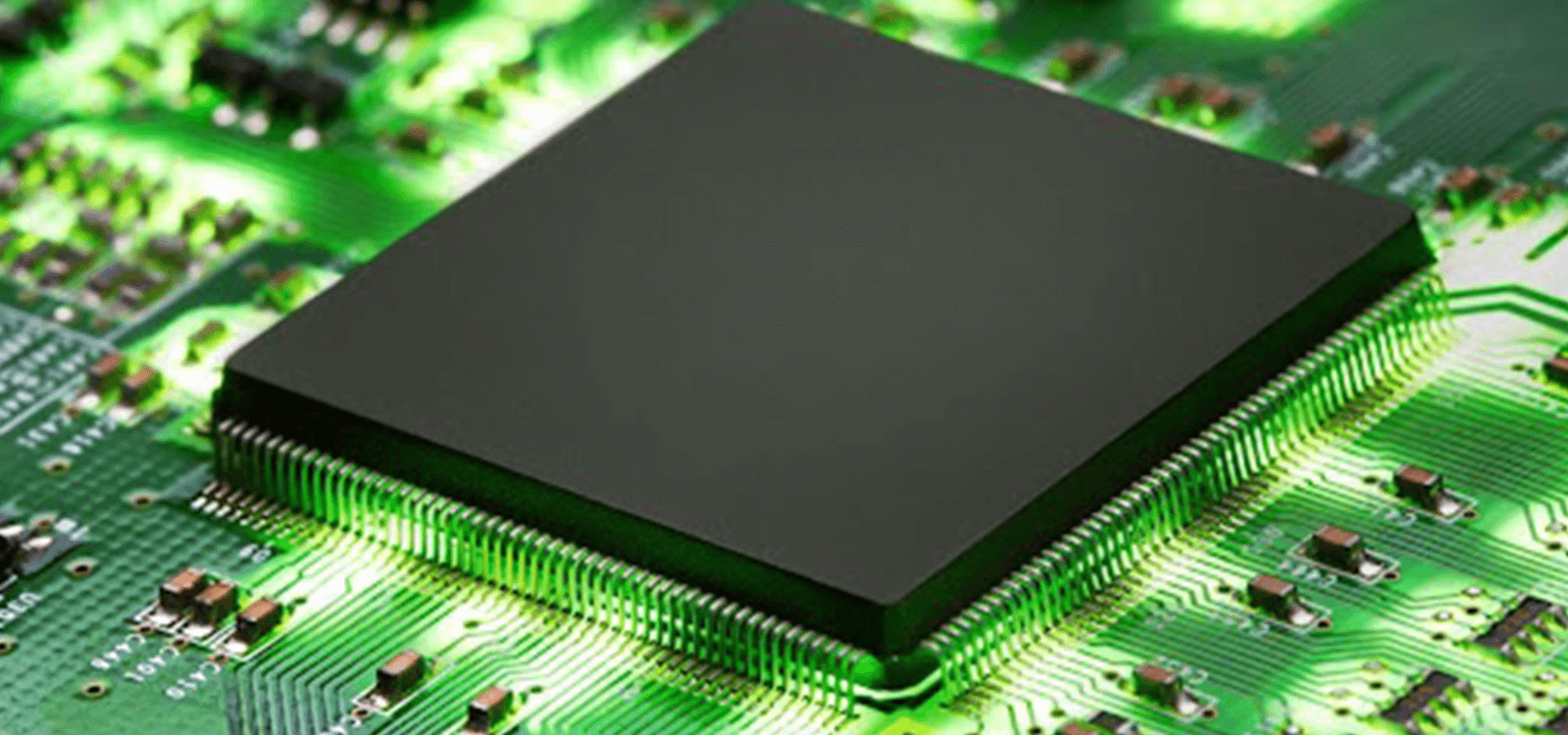
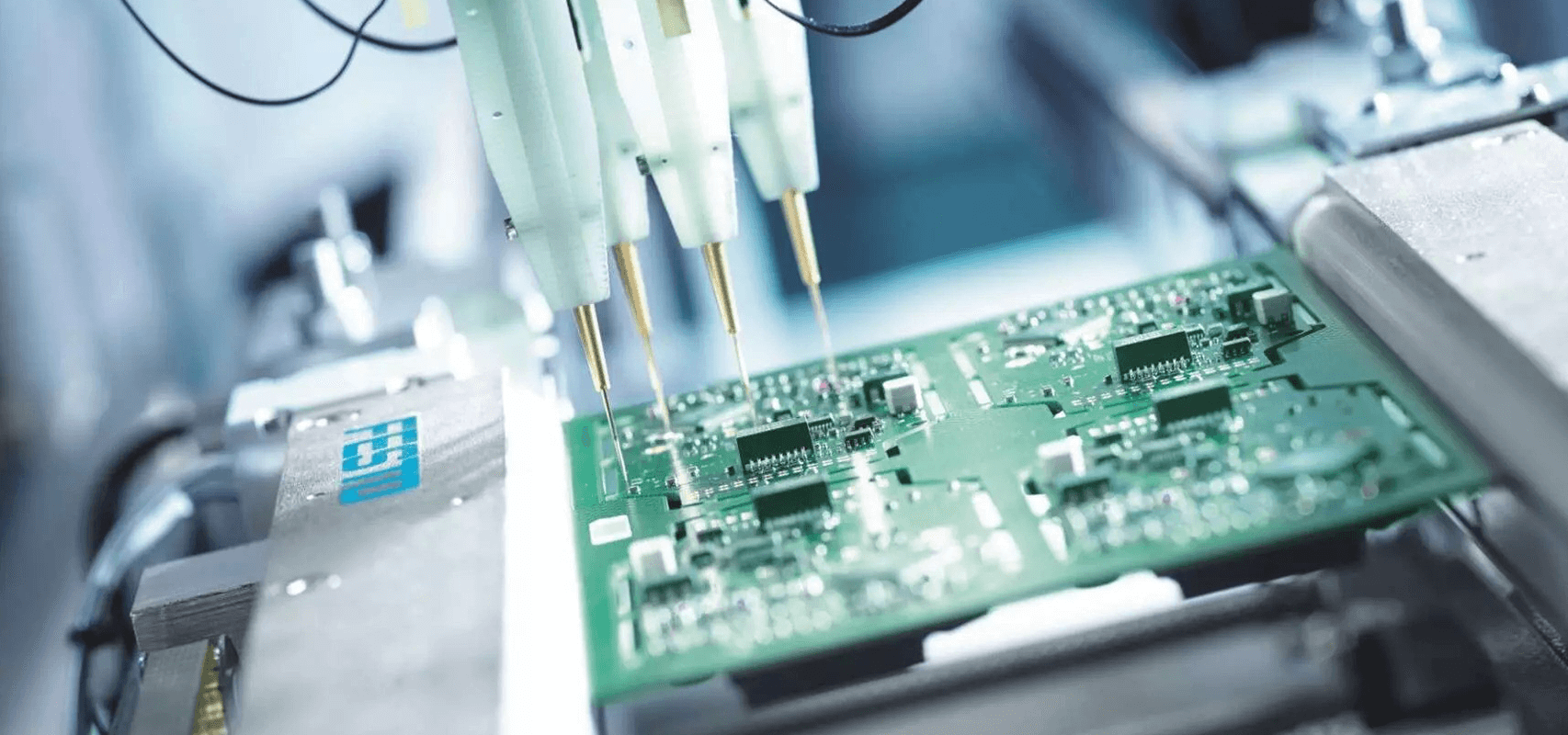
PCB is vital for creating electronic devices, providing a structured platform for interconnecting electronic components. However, technological advancement led to space constraints in PCB, as multiple components must be placed in a smaller space. Hence, DFT (Design for Testability) comes into the picture to improve the testability of PCB, increasing the product’s overall lifecycle.
During the PCB hardware design phase, DFT ensures efficient testing by incorporating necessary test points on the PCB for each component and connection. It helps to identify faulty components and shorted/open connections post-production. So, the better testability of PCB hardware ensures a functional hardware and improves the reliability and performance of the final product.
Key Principles of DFT in PCB Design
Accessibility of Test Points
During the PCB hardware design phase, strategic placement of test points is crucial for accessibility during testing. This ensures efficient testing processes, reducing time and effort for issue identification.
Testability as a Design Goal
Considering testability as a primary design goal from the outset ensures that the PCB board is inherently designed for efficient testing. This proactive approach minimizes the need for redesign and modifications later in development.
Built-in Self-Test (BIST)
Incorporating self-testing mechanisms, such as Built-in Self-Test (BIST), within the PCB allows the board to perform self-diagnostic tests. This enhances fault coverage, reducing dependency on external test equipment.
Fault Coverage and Diagnosis
DFT aims for comprehensive fault coverage and easy diagnosis. It identifies and covers potential faults, providing clear information about fault location and nature for efficient debugging.
Minimization of Test Points’ Impact on Signal Integrity
While placing test points strategically, minimizing their impact on signal integrity is crucial, ensuring the introduction of test points doesn’t compromise PCB functionality.

Advantages of Implementing DFT in PCB Design
Improved Product Reliability
Early detection of faults and a proactive approach to testing contribute to the enhanced overall reliability of the final product. By addressing potential issues during the design phase, DFT ensures that the PCB board meets the highest standards of performance and longevity.
Cost Reduction
Streamlined testing processes and early fault identification result in substantial cost reductions. By minimizing testing time and the need for extensive debugging, DFT contributes to a more cost-effective development lifecycle.
Accelerated Time-to-Market
Proactively implementing DFT shortens development cycles, providing a competitive edge in the market. The efficient testing facilitated by DFT enables faster iterations and quicker product launches, contributing to an accelerated time-to-market.
Brand Reputation Enhancement
Products born out of effective DFT practices inherently possess higher quality and reliability. This positively impacts brand reputation, fostering trust among consumers and stakeholders. A strong brand reputation, in turn, contributes to sustained market success and customer loyalty.
Challenges in Implementing DFT
Space Constraints
In an era where miniaturization is a driving force, optimizing testability in small PCB spaces presents a significant challenge. Balancing the need for efficient testing with the demand for compact designs requires careful consideration and innovative solutions.
Technological Complexity
The rapid evolution of technologies introduces a continuous challenge for PCB designers to stay updated on the latest DFT strategies and tools. Navigating technological complexity necessitates ongoing education and a commitment to adapting design practices to align with emerging trends.
Skill Requirements
Implementing advanced DFT techniques may require specialized skills that not all design teams possess. Addressing this challenge involves fostering a culture of continuous learning and seeking external expertise to ensure proficiency in cutting-edge DFT methodologies.
Precision and Signal Integrity
Maintaining signal integrity is crucial in high-quality PCB hardware, especially those used in high-speed data transfer. Implementing DFT features without compromising signal quality can be challenging, as additional test points and circuits may introduce impedance mismatches and stubs causing signal reflections.
High-Density Packaging
High-quality PCBs often involve high-density packaging to accommodate numerous components in a confined space. Integrating DFT in such densely packed designs requires careful planning to ensure that test access points are strategically placed without interfering with other critical components.

Future Trends and Innovations in DFT for PCB Design
AI-Enhanced Testing
Integrating Artificial Intelligence (AI) in testing processes is a promising avenue for the future of DFT. AI can provide more intelligent and adaptive testing, enhancing fault detection and overall test efficiency.
IoT Integration
With the growing prominence of the Internet of Things (IoT), DFT solutions tailored to the unique challenges posed by IoT device designs are expected to emerge. These solutions will address the specific testing requirements of interconnected and sensor-laden devices.
Advanced Simulation Tools
The development of more advanced simulation tools is anticipated to revolutionize DFT in PCB design. These tools will offer more accurate pre-production testing, enabling designers to identify and address potential issues more precisely.
Also Read: Understanding the Difference: Hardware Design vs. PCB Design
Concluding Remarks
The role of DFT in designing high-quality PCBs is paramount in the ever-evolving landscape of electronic devices. As electronic devices continue to advance, DFT is a current necessity and a pathway to the future. Its precision, efficiency, and adaptability offer PCB design solutions to the challenges, defining the next generation of high-quality PCB design.
Tessolve helps semiconductor companies to design PCBs meeting DFT requirements. We work closely with manufacturers to incorporate the DFT rules into the PCB Constraints manager and ensure PCBs are designed right at the first time.


