Our team of Design for Testability experts can help increase IC test coverage, yields and quality.
Overview
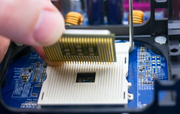
Continuously shrinking process nodes have introduced new and complex on-chip variation effects creating new yield challenges. Combined with ever-increasing design complexity with multiple memories, mixed signal blocks and IPs from multiple vendors crammed into a single SoC, Design for Test (DFT) implementation and Production Test signoff has become a major challenge. The Tessolve asureDFT services suite helps you to overcome these challenges by establishing a DFT strategy that delivers improved DFT execution quality and reduced time-to market.
Services

Implementing Scan ( Compression/ non-compression ) implementation with industry standard tools

ATPG (stuck-at, at-speed, SDD, Path delay, new faults based on the technology and strategy) vector generation, Covergae analysis, Pattern (verilog, wgl) simulation (Gate Level Simulations (unit-delay, extracted dealy with sdf)

Memory BIST implementation, Simulation & Vector preparation for good simulation and repair flow with fault Injections with industry standard EDA tools
- Experienced professionals can support on the in-house tool based implementation/verification for our customers.
- Logic BIST
- IEEE 1149.1, IEEE1149.6 compliance test controllers (JTAG)
- Ensuring the design integrity on pre and post DFT by Formal Verification
- ATE support on pattern stabilization, split lot analysis / Diagnosis of Structural (scan, mbist) failures
Off-the-Shelf DFT Components
- JTAG TAP based test controllers and verification frame works (JTAG, IEEE 1149, TAP and its customized Instructions)
- Test suites for Verifying BSCAN and generating tests for DC parametric tests (No dependencies with EDA Tool)
- Generating Tester compatible vectors for Post Si validation (ATE)
- Format conversions with ATE logs for diagnosis
Design for Testability Training
- DFT Strategy/Structural Testing with testmode STA needs
- Exclusive trainings on JTAG, BSCAN, SCAN, MBIST
- Customized contents for customer requirements
Design for Testability Methodology Services
- Development of DFT methodology
- Assessment of existing DFT methodology
Benefits of Design for Testability
- Reduced overhead due to trained skills being available – No need to hire expensive DFT resources
- End-to-end support – From design to silicon
- Off the shelf components – Reduce DFT turnaround times
- Training support – Bridge the gap in experience levels; Remote support from Tessolve office to resources at customer sites
Benefits of Design for Testability

End-to-end DFT for a consumer SoC
Tessolve was tasked with scan implementation, verification and pattern delivery for a complex consumer SoC which had a flop count of around 1.5 million. Memory BIST (MBIST) also had to be performed for 400+ memory instances. The stuck at and at-speed coverage analysis targets were set at 99% and 85% respectively.

Implementing DFT for a network SoC
When a customer urgently needed a team of engineers for DFT implementation and execution of its network SoC, they turned to tessolve for help. After the design had been analyzed and the DFT implementation effort had been estimated, Tessolve had to execute DFT DRC for Scan and implement compression and the stuck-at coverage target for the SoC was an aggressive 99.8%
Find Out More
Contact one of our consultants today to discuss your requirements.
No hard sales, just pertinent questions to understand your needs and to discuss how we may be able to help.
Alternatively contact one of our Local Sales Offices.


