Semiconductor companies predominantly drive the development and implementation of 5G technology. 5G technology offers lower latency, faster data rates, and a more comprehensive range of applications, promising a significant transformation in communication.
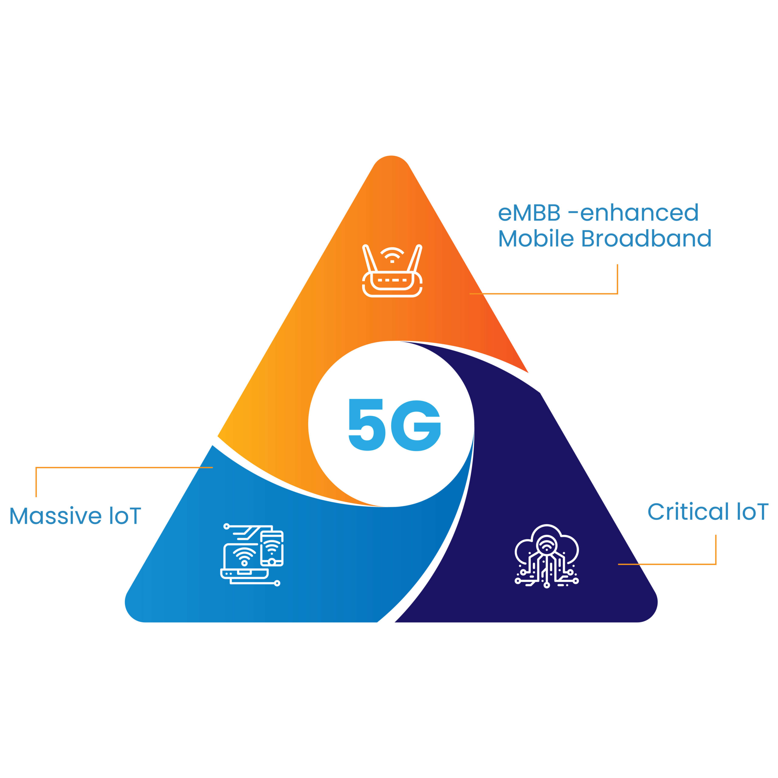
The rationale for 5G development is to expand the broadband capability of mobile networks, and to provide specific capabilities not only for consumers but also for various industries and society at large, hence unleashing the potential of the Internet of Things (IoT).
However, a robust New Product Introduction (NPI) process is imperative to efficiently and expeditiously bring sophisticated 5G devices to the market. This is where semiconductor engineering services firms such as Tessolve play a crucial role.
As 5G and future 6G networks incorporate Non-Terrestrial Networks (NTNs) into their design, pushing past the boundaries of terrestrial-based infrastructure, the impact of NTNs will become even more significant. Because of their ability to connect the unconnected (theoretically anywhere in the world), NTNs continue to play an increasingly prominent role in wireless communications, enabling ubiquitous connectivity and supporting emerging technologies like autonomous vehicles and IoT.
With the advent of 5G Non-Terrestrial Networks (NTNs), the landscape of satellite phone availability is undergoing a revolutionary transformation. Soon, satellite service will be accessible to billions of mobile phone subscribers worldwide, ushering in a new era of connectivity.
Over the past year, some of the world’s largest semiconductor manufacturers have announced new chipsets for satellite IoT and direct-to-handset connectivity using 5G non-terrestrial network (NTN) standards. The chipsets are among the first to leverage 3GPP protocols in Release 17, which was the first mobile industry standard designed to include satellite.
It’s remarkable enough to see chipmakers more involved in satellite communications. But what is essentially driving major players in the mobile industry toward satellite is standardization around 3GPP’s NTN standards. In the case narrowband (NB) use cases, like IoT and SOS messaging, the standard is NB-IoT or IoT-NTN. For broader use cases, 3GPP supports New Radio (NR)-based satellite access technology, which currently supports higher data rate applications, like two-way text and data, in the sub-6 GHz bands. The NR-NTN standard is designed to be forward-compatible and eventually adapt to higher frequency bands used in satellite communications, like Ka.
Future of Semiconductor Technology in 5G Era
The future of semiconductors in the 5G era looks promising, with several innovations on the horizon:
- Open-source hardware is disrupting the market and changing how companies think about design.
- IoT increases the demand on cost-effective semiconductors.
- 5G accelerates demand for high-performance computing devices.
- Artificial Intelligence (AI) Integration: AI is expected to significantly optimize 5G network performance. Semiconductors with embedded AI capabilities will enable more innovative and efficient networks.
- Quantum Computing: Although still in its infancy, quantum computing has the potential to solve complex problems in 5G network design and optimization.
- Flexible Electronics: Advancements in semiconductor materials and fabrication techniques will benefit the development of flexible and wearable devices, enabling new applications in healthcare, entertainment, and beyond.
The Role of Semiconductors in 5G Technology
Semiconductors are essential to the functioning of 5G networks, serving as the building blocks for various devices and infrastructure. They are used in:
- Base Stations: Advanced semiconductor chips are crucial for the enhanced processing capabilities required in 5G base stations, which manage increased data loads and complex signal processing.
- Mobile Devices: Smartphones and other mobile devices leverage powerful semiconductors to support 5G connectivity, ensuring faster download and upload speeds.
- IoT Devices: 5G will significantly benefit the Internet of Things (IoT) ecosystem, and semiconductors enable these devices to communicate efficiently and reliably.
The Semiconductor Design Revolution
Meeting 5G’s demands requires a complete overhaul of chip design. Below are some top trends to watch:
- Millimeter Wave Magic: 5G utilizes millimeter waves, which offer incredible speed but have a shorter range. This necessitates a new generation of antennas and radio frequency (RF) components specifically designed for these frequencies.
- Rise of the Machines: The Internet of Things (IoT) explosion, fueled by 5G, demands low-power, high-performance chips specifically designed for these smaller, battery-powered devices.
- AI on the Edge: Artificial intelligence (AI) is inching closer to the data source, with “edge computing” becoming a reality. This needs chips capable of on-device AI processing for quicker response times.
Advances in Semiconductor Design for 5G
The demands of 5G technology have led to significant advancements in semiconductor design, characterized by the following trends:
- Miniaturization and Integration: One critical trend in semiconductor design is the push towards more minor, more integrated chips. As 5G devices require enhanced functionality without increasing size, semiconductor manufacturers focus on miniaturization and integrating multiple functions into single chips. This trend is evident in developing System-on-Chip (SoC) designs, which integrate processors, memory, and radio frequency (RF) components on a single chip.
- Enhanced Performance and Efficiency: 5G technology necessitates higher performance and energy efficiency from semiconductors. Innovations in materials, such as adopting gallium nitride (GaN) and silicon carbide (SiC), are driving these improvements. GaN and SiC semiconductors offer superior power handling and efficiency, making them ideal for high-frequency, high-power 5G applications.
- Advanced Packaging Technologies: Advanced packaging technologies are being developed to meet the stringent requirements of 5G. Techniques like 3D stacking and chipset integration were becoming more prevalent, allowing higher performance and reduced latency. These packaging methods enable closer proximity of components, which is critical for the speed and efficiency of 5G networks.
- Market Growth and Economic Impact: The 5G semiconductor market is undergoing healthy growth, driven by the expanding deployment of 5G networks globally. According to a report by MarketsandMarkets, the 5G chipset market is projected to grow from USD 1.9 billion in 2020 to USD 22.4 billion by 2026 at a compound annual growth rate (CAGR) of 48.7%. This explosive growth underscores the critical role of semiconductors in the 5G revolution.
Furthermore, the economic impact of 5G is substantial. A study by IHS Markit estimates that 5G will enable USD 13.2 trillion in global economic output by 2035, with the semiconductor industry playing a pivotal role in this economic transformation.
The Challenges of 5G NPI
During the New Product Introduction (NPI) phase, every semiconductor design company involved in developing 5G products faces several challenges, including:
- Increasing Complexity: The complexity of 5G technology encompasses advanced packaging methods, millimeter wave (mmWave) integration, and intricate radio frequency (RF) designs, necessitating a high level of skills to navigate the design, test, and manufacturing processes.
- Faster Time-to-Market: Quick product development cycles are necessary in the 5G competitive scenario. To take advantage of the early adopter market, businesses must launch their products swiftly. Shifting to an IP-centric design methodology can help you accelerate design and reduce costs by enabling more efficient IP reuse.
- Integration Challenges: Digital signal processors (DSPs), field-programmable gate arrays (FPGAs), and bespoke silicon are just a few of the components that 5G systems must combine. For product development to be successful, these components must perform and integrate seamlessly with one another.
- Test and Validation: Testing and validating 5G products require specialized equipment and expertise to handle the high frequencies and complex protocols involved.
- Thermal Management: The increased power density in 5G semiconductors generates significant heat, requiring advanced thermal management solutions.
- Signal Interference: The higher frequencies in 5G are more susceptible to signal interference, necessitating robust RF design and filtering techniques.
- Security: As 5G networks handle more data, ensuring the security of semiconductor components against cyber threats is crucial.
How Tessolve’s NPI Expertise Can Help
A prominent provider of semiconductor engineering services in the United States, Tessolve provides a full range of NPI services that can expedite the development of 5G products. Among these services are:
- Services for Design for Manufacturability (DFM): Tessolve’s DFM specialists can assist a semiconductor design company in recognizing and resolving possible manufacturability problems at an early stage of the design process. This can significantly lower the possibility of manufacturing delays and rework.
- Design for Test (DFT) Services: Tessolve’s Design for Test (DFT) services can assist in guaranteeing effective and economical testing of 5G equipment by introducing DFT approaches early in the design phase. This involves writing automation scripts, establishing test frameworks, and drafting test plans.
- Prototyping and Pilot Build: Before committing to high-volume production, businesses may validate their ideas and find any faults with Tessolve’s prototyping and pilot build capabilities. Because less expensive rework is required, this can save both time and money.
- Test Engineering Services: Electrical, functional, and compliance testing are just a few of the many test engineering services that Tessolve provides. The business possesses the knowledge and tools necessary to manage the intricate testing specifications of 5G products.
- Manufacturing Engineering Services: Tessolve can assist businesses in ensuring a seamless transition from prototype to high-volume production by offering its manufacturing engineering services. This includes creating plans for the manufacturing process, maximizing production yields, and offering continuous assistance with production.
- Compliance and Interoperability Testing: Robust testing and verification services ensure that 5G devices and networks meet stringent performance and regulatory standards. These services encompass compliance testing, which ensures adherence to 5G standards and regulations, and interoperability testing, designed to guarantee seamless operation among various devices and networks. By leveraging such services, reliable, high-performance 5G technology can be brought to the market, thus realizing the full potential of this groundbreaking wireless communication standard.
Benefits of Partnering with Tessolve for 5G NPI
Semiconductor businesses can get many advantages by collaborating with Tessolve to meet their 5G NPI requirements. These benefits include:
- Decreased Time-to-Market: Businesses can take advantage of early market opportunities by bringing their 5G products to market more quickly, thanks to Tessolve’s experience and simplified NPI process.
- Enhanced Product Quality: Tessolve’s emphasis on DFM and DFT contributes to the highest standards of product manufacturing for 5G goods. This lowers the possibility of field malfunctions and product flaws.
- Reduced Costs: Tessolve can help businesses avoid expensive rework and delays by spotting and resolving possible problems early in the NPI process. Tessolve’s effective testing techniques can also contribute to a decrease in total test expenses.
- Access to Expertise: Tessolve has a team of experienced engineers with deep knowledge of 5G technology and the NPI process. By partnering with Tessolve, companies gain access to this expertise, which can be invaluable for navigating the complexities of 5G product development.
Tessolve: Your Partner in 5G Success
As a leading semiconductor systems integrator and a recognized semiconductor leader, Tessolve is well-positioned to help companies develop and launch successful 5G products. With its comprehensive suite of NPI services and deep expertise in 5G technology, Tessolve can be a valuable partner for any company looking to streamline its 5G product development process.
Tessolve: Addressing the Needs of Diverse 5G Applications
Tessolve, a semiconductor company in USA understands the unique challenges and requirements of different 5G applications. The company’s NPI services are tailored to address the specific needs of various industry segments, ensuring that semiconductor companies can develop products optimized for their target markets. For instance, Tessolve’s expertise in high-speed design and signal integrity is crucial for developing the complex RF components needed for automotive radar systems and communication modules in self-driving cars. Similarly, the company’s knowledge of low-power design principles is valuable for creating energy-efficient processors for battery-powered wearable devices used in the healthcare sector.
Also Know: How Does Advancement in PCB Design Improve the Connectivity and Power Efficiency in IoT Devices?
Let’s Conclude
The advancement of 5G technology has opened promising prospects for semiconductor companies. However, effectively navigating through the New Product Introduction (NPI) process necessitates a strategic approach and specialized expertise. By collaborating with Tessolve, firms can capitalize on the company’s NPI proficiency to mitigate risks, expedite time-to-market, and guarantee the triumph of their 5G products. Additionally, the rise of 5G is reshaping the semiconductor industry by driving demand for advanced chips, edge computing, new materials, and expanded IoT applications, necessitating increased collaboration across sectors.


