A well-designed PCB (Printed Circuit Board) is the cornerstone of a dependable and valuable gadget in the world of electronics. However, a PCB does more than merely join parts together; it is essential for controlling electrical signals and keeping unsightly electrical bugs from destroying your circuit. The two main obstacles that PCB design engineers must overcome are electromagnetic interference (EMI) and crosstalk.
This article explores efficient ways to reduce EMI and crosstalk in your next PCB hardware design as it dives into the world of PCB layout techniques.
Understanding the Threats: Crosstalk and EMI
-
- Crosstalk: Imagine two parallel lines on a PCB, each carrying electrical impulses. A fluctuating voltage on one line can induce a small current on the other due to the inherent capacitance between these traces. This unintentional connection, known as crosstalk, can lead to data corruption and circuit malfunctions, particularly in high-frequency or vulnerable circuits.
- Electromagnetic Interference (EMI): Electromagnetic Interference (EMI) is a well-documented phenomenon in electronic systems. Whenever an electrical current flows, it generates a magnetic field, and each change in voltage produces an electric field. These fields, collectively known as EMI, have the potential to disrupt the operation of nearby electronic devices. Furthermore, external sources of EMI can induce unwanted electrical currents within PCBs, posing a risk of damage to the delicate circuitry.
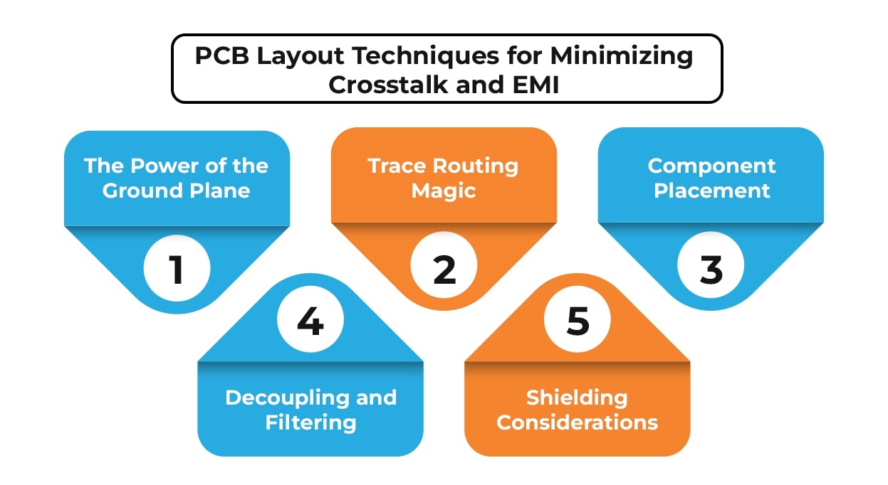
PCB Layout Techniques for Minimizing Crosstalk and EMI

Fortunately, a well-crafted PCB layout strategy can significantly reduce crosstalk and EMI. Here are some key techniques to consider:
1. The Power of the Ground Plane
The ground plane is an often overlooked yet essential element in PCB design. In addition to providing a low-impedance path for returning current, a wide and continuous ground plane also serves as a vital reference point for signals. By minimizing the loop area of the current, we can effectively reduce the level of radiated electromagnetic interference. The following tips will help you get the most out of your ground plane:
-
- Optimize Terrain: Use as much space as possible on your PCB design for the ground plane.
- Multiple-layer Magic: Dedicated ground planes on multi-layer PCBs enable improved signal separation and noise reduction.
- Strategic Stitching: If you need to split the ground plane for routing reasons, use stitching vias to join the divided areas. These vias serve as brief, low-impedance channels for the flow of current.
2. Trace Routing Magic
-
- Spacing is Key: Make sure there is enough room between signal traces. Wider gaps minimize crosstalk and capacitive coupling because they lower the capacitance between them. Adhere to the PCB design guidelines that you have selected for recommended trace spacing based on trace width and layer thickness.
- Differential Pairs: Allocate tightly spaced, parallel lines for high-speed differential signals. This guarantees that any electromagnetic interference (EMI) detected by a single conductor is common-mode noise, which the differential receiver will reject.
- Controlled Impedance: To obtain a controlled characteristic impedance, keep the trace width of necessary signals constant. This reduces reflections that may result in EMI and guarantees correct signal integrity.
- Softening the Bends: Avoid abrupt 90-degree turns in traces. These may cause unintentional reflections and capacitance. When feasible, use mitered bends or rounded corners.
3. Component Placement
-
- Separation Is Essential: On the PCB, physically divide the high-speed and low-speed signals. As a result, there is less possibility that high-speed signals may cause noise in low-speed ones.
- Analog vs. Digital: Separate circuitry that is analog from that that is digital. Digital circuits’ switching characteristics can produce noise that interferes with delicate analog components. To establish physical barriers between these realms, use the ground plane or designated slots.
- Best Path, Shortest Path: Give small trace lengths priority, particularly for high-speed signals. Shorter traces reduce emitted EMI by minimizing loop regions.
4. Decoupling and Filtering
Capacitors used for decoupling and filtering serve as tiny charge reservoirs that supply ICs with a localized source of current while obstructing the transmission of noise onto the power supply lines. Observe these pointers for a successful decoupling:
-
- Position decoupling capacitors in close proximity to the ICs’ power pins.
- Expand the range of noise frequencies you target by using numerous capacitors with varying values.
- If you want to filter high-frequency noise on power supply cables, think about using ferrite beads.
5. Shielding Considerations
Although shielding can be an effective method of reducing electromagnetic interference (EMI), its usage should be considered carefully because of its effects on cost and size. Techniques for shielding include:
-
- Metal enclosures or cans: These can cover whole PCB parts or delicate components.
- Grounding strips: Wide copper strips routed around loud areas can serve as grounding strips, helping to reduce EMI radiation.
Also Read : A Comprehensive Guide to Wireless Testing Strategies
Conclusion
Through the application of these PCB layout techniques, PCB design engineers can effectively minimize EMI and crosstalk in their designs. This contributes to achieving regulatory compliance for electromagnetic emissions while also guaranteeing dependable operation. Recall that for your PCB design in USA or anywhere else in the world, a well-thought-out PCB layout is an investment that pays off in terms of increased performance, decreased chance of malfunctions, and a smoother route to production.
At Tessolve, we offer cutting-edge solutions in PCB design, manufacturing, and testing, helping businesses overcome challenges like EMI and crosstalk with innovative strategies. With extensive expertise in semiconductor and hardware engineering, we ensure robust designs that meet industry standards. Partner with us to bring your ideas to life and achieve excellence in your electronics projects.


