In the rapidly changing realm of printed circuit board (PCB) design, selecting an appropriate stack-up is not merely a technical choice; rather, it is a pivotal determinant that can significantly impact the overall performance, manufacturability, and cost efficiency of your project. Whether you’re working on a PCB design for a straightforward two-layer board or venturing into the complexities of a high-density, multilayer design, optimizing your PCB stackup is essential for ensuring signal integrity, minimizing electromagnetic interference (EMI) and noise and improving thermal management. A well-thought-out stackup can even streamline the manufacturing process and enhance the long-term reliability of your product.
In this comprehensive guide, we will dive into the details of what a PCB stack-up is, why it plays such a pivotal role in your design, and practical strategies for optimizing it to achieve a successful, high-performing design.
Get in touch
What Is PCB Stackup?
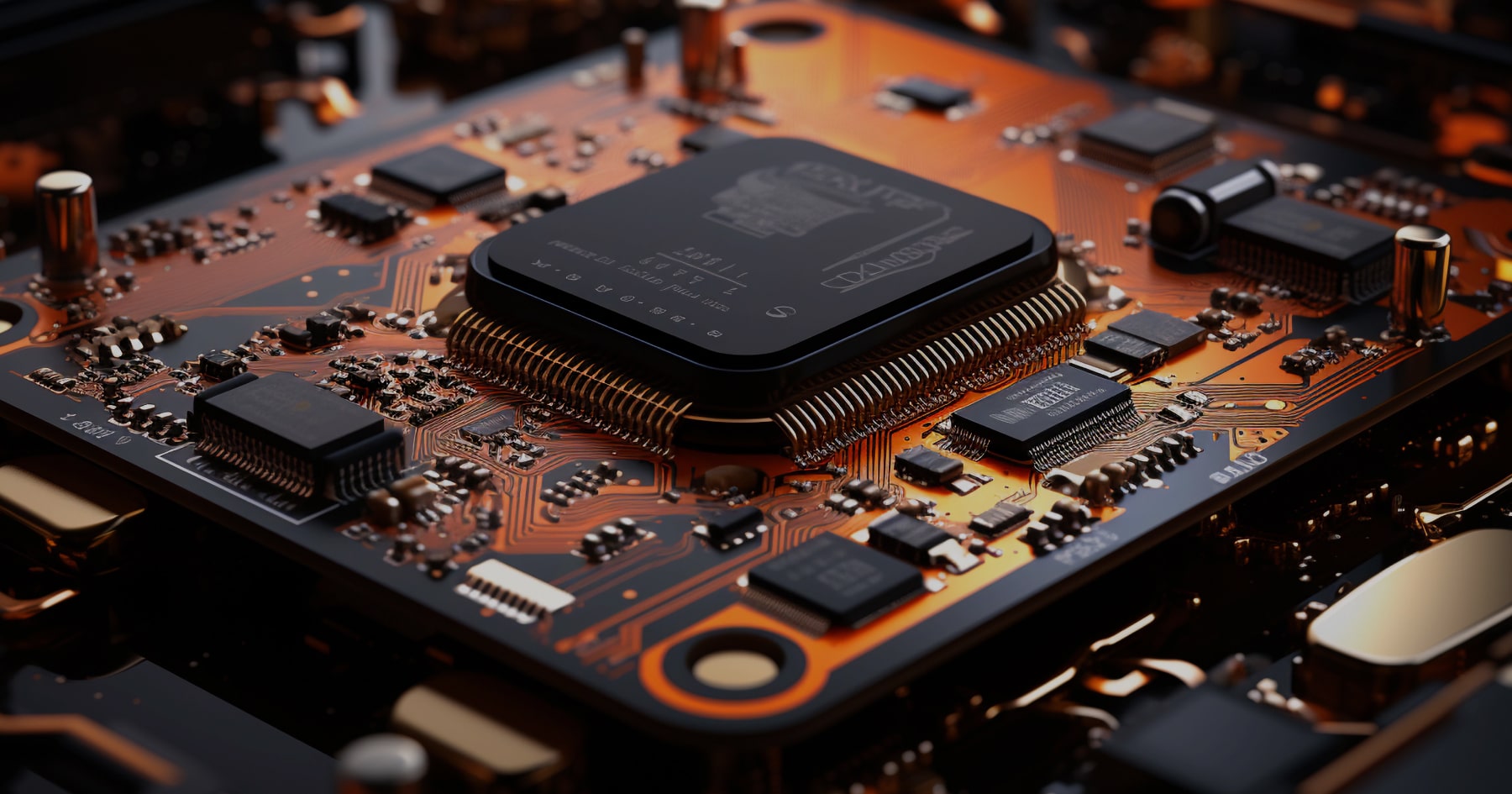
A PCB stackup refers to the arrangement of layers within the PCB design, each serving a specific function. Depending on the design’s complexity, the number of layers can range from two to dozens. Typical PCB stackup layers include signal, ground, power, and dielectric layers that electrically isolate these layers.
Multilayer PCBs are common in modern electronics, allowing for compact designs supporting high-performance components. Understanding how to configure the layers properly ensures the final product operates efficiently.
Why Stackup Selection Is Important
The stackup configuration plays a crucial role in the following areas:
- Signal Integrity: High-speed signals are sensitive to interference. A well-designed stackup mitigates issues like crosstalk and reflections, enhancing signal integrity by isolating critical signal layers and ensuring impedance control.
- Thermal Management: Optimized stackups help dissipate heat, preventing hot spots and ensuring reliable long-term operation.
- Cost Efficiency: The number of layers directly influences production costs. A well-optimized stackup minimizes unnecessary layers while maintaining functionality, keeping manufacturing costs in check.
- Electromagnetic Interference (EMI): Proper stackup design can significantly reduce EMI, especially in high-frequency circuits, by providing effective shielding and routing.
Key Factors in Stackup Selection
When designing your PCB, keep the following factors in mind:
1. Layer Count and Configuration
The number of layers in your PCB design depends on the complexity of your design. For simpler applications, a two-layer PCB may be enough. However, high-speed designs or applications requiring advanced power distribution often require four or more layers.
Multilayer PCBs typically dedicate specific layers for power and ground planes, which not only enhance signal integrity but also simplify routing.
2. Impedance Control
Maintaining consistent impedance is essential in high-speed designs. The thickness of the dielectric layer, along with the use of adjacent ground planes, helps to control impedance, reducing signal degradation. This can be critical in RF circuits, where a mismatch in impedance could compromise performance.
3. Material Selection
PCB material affects both electrical and thermal performance. Common materials like FR4 are suitable for many applications, but higher-performance boards may require specialized materials like PTFE or Rogers laminates for improved signal integrity at higher frequencies.
4. Signal Layer Distribution
Carefully distributing signal layers in your stackup is vital for noise reduction and signal integrity. Placing signal layers between ground planes helps reduce crosstalk and noise. Additionally, reducing trace lengths and minimizing via use further improves signal performance.
5. Thermal Considerations
Heat management is a key factor, particularly in high-power designs. A well-designed stackup will manage heat by distributing it evenly or routing it away from hot spots. Choosing thermally conductive materials can further enhance performance.
Common PCB Stackup Configurations
PCB stack-ups refer to the arrangement of layers within a printed circuit board. Each layer can be a signal layer (for carrying electrical signals) or a power plane (for distributing power or ground). The number of layers in a stackup directly impacts the board’s complexity, cost, and performance.
- 4-layer stackup: This is a common configuration for low-speed designs, often consisting of two signal layers sandwiched between two power planes. It provides a balance of signal integrity and cost.
- 6-layer stackup: When more signal layers or power planes are needed, a 6-layer stackup is often employed. This configuration can accommodate higher-density designs or those requiring additional power distribution.
- 8-layer stackup: An 8-layer stackup is a popular choice for high-speed designs or those demanding significant power distribution. It offers ample space for signal routing and power planes, helping to minimize crosstalk and impedance mismatches.
- 10-layer stack-up: This configuration is considered for very complex designs or those requiring an extensive number of signal layers. It provides maximum flexibility for routing intricate circuits and distributing power efficiently.
It’s important to note that while the number of layers is a key factor, other considerations like layer thickness, dielectric material, and placement also influence board performance. The optimal stackup for a specific design depends on factors such as the circuit’s complexity, speed requirements, and manufacturing constraints.
Partnering with Tessolve for Advanced PCB Stackup Optimization
Tessolve’s expertise in PCB hardware design and manufacturing aligns seamlessly with the principles outlined in the guide. As a leader in semiconductor solutions, Tessolve supports the full product lifecycle, including advanced hardware design services and multilayer stackups, which are essential for maintaining signal integrity, thermal management, and cost efficiency. With our comprehensive design verification and test engineering services, Tessolve ensures that even the most complex designs meet stringent performance and manufacturability standards. Therefore, by partnering with us, you can optimize your PCB stackup to enhance your product’s performance while keeping production costs in check.
Let’s Sum Up
Choosing the right stackup is a critical part of PCB hardware design, affecting everything from signal integrity to manufacturing costs. By carefully considering factors like layer count, impedance control, and material selection, you can create a PCB design that meets your design’s technical requirements while staying within budget. With a well-optimized stackup, you can ensure that your PCB performs reliably, remains cost-effective, and is easier to manufacture.


