Due to semiconductor advancement, the digital world is demanding more and more electronics products from engineers. This makes the engineering job more complex and bigger in scope. That’s where AI has revolutionized the chip industry by playing a pivotal role in modern-day chip design.
Electronic Design Automation (EDA) tools are software applications that VLSI chips design engineers utilize during the design and development of electronic systems, including chip design. AI-powered EDA tools enhance and automate the various stages of the design process by leveraging AI methodologies, such as machine learning and deep learning. These tools can analyze large datasets, recognize patterns, and make data-driven decisions. This aids engineers in exploring design spaces more effectively and addresses the growing complexity of modern electronic systems. This blog will delve deeper into the need for AI in chip design, benefits, and applications.
What Is the Need for AI in Chip Design?
The complexity of chip design is increasing daily due to advancements in semiconductor technology, such as advanced process nodes, quantum dots, heterogeneous integration, etc. This has led to unprecedented challenges for VLSI hardware design engineers. That’s where AI has emerged as a powerful solution, aiding in silicon quality and productivity in designing smaller PCB designs.
Engineers face numerous possibilities while designing, verifying, and testing the chip for new-age electronics design. So, they find the best-case scenario for better power, performance, and area, as they need to bind numerous transistors into one design. Incorporating AI has increased chip design productivity, quality, and efficiency and reduced design costs.
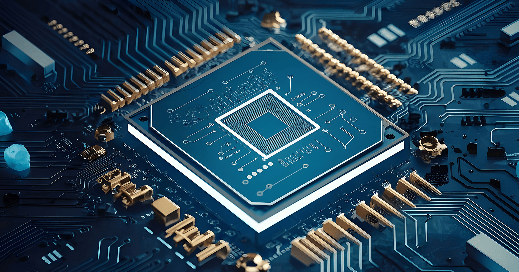
Introducing AI-Powered EDA Tools
EDA is a set of software, hardware, and essential services that are used for chip design and semiconductor devices. However, due to billions of connections and multiple teams, EDA tools are essential for VLSI design service providers in hardware creation. This performs three essential duties: simulation, design, and verification. This simulated world is where chips are analyzed to meet intended performance before making it to the real world. In addition, EDA tools have evolved with artificial intelligence.
Benefits of Using AI-Powered EDA Tools for Chip Design
Power and Performance Optimisation
AI aids in simultaneously optimizing chip designs for power consumption and performance, a critical factor in today’s electronics. Machine learning algorithms can assess and forecast how various design decisions will affect power and performance, which can result in more energy-efficient solutions.
Design Space Exploration
AI makes it possible to investigate the design space in greater detail. AI-driven technologies can find the best trade-offs and solutions by simultaneously considering many design aspects and settings. These are trade-offs that may be difficult for human designers to manually examine.
Managing Big Data in Design
A large amount of data is produced during the simulation, verification, and testing phases of the semiconductor design process. AI technologies may analyze large datasets quickly, which can also be used to derive insights from the data and make data-driven decisions that enhance design quality.
Customization and Specialisation
AI makes it possible to develop highly customized chips for certain applications. Artificial intelligence (AI) driven design tools can customize chips to individual algorithms’ unique requirements, enhancing overall system performance in domains like AI, where specialized hardware accelerators are critical.
Applications of AI in Chip Design
Design Space Exploration
AI-powered EDA tools revolutionize design by optimizing performance, power, and area (PPA). This analyzes data and identifies patterns, helping to achieve a balance and meet specifications. These tools excel in navigating the multifaceted design space, aiding informed decisions on power, performance, and area trade-offs. This proves invaluable in achieving VLSI physical design goals amid competing constraints. AI-powered EDA tools leverage machine learning to identify optimal design configurations, accelerating exploration and allowing designers to focus on efficient solutions.
Physical Design Automation
AI-powered EDA tools automate the physical design by optimizing the components’ arrangement. This enhances signal integrity, minimizes power consumption, and manages thermal considerations. Its predictive analysis is crucial in achieving timing closure by proactively addressing issues early in the design phase. This reduces the likelihood of last-minute adjustments.
Timing Closure and Verification
AI-powered EDA tools encompass predictive analysis, which extends to critical timing closure tasks. It forecasts potential timing issues, proposing preemptive solutions to streamline the process, reducing traditional time and effort.
AI’s role in VLSI board design verification utilizes machine learning techniques to enhance the process’s robustness. This recognizes complex patterns and potential design errors, making verification more efficient. This minimizes the risk of overlooking critical issues. In debugging and error correction phases, AI-powered EDA tools play a crucial role by automating the identification and correction of errors. This minimizes manual efforts, ensuring an efficient and reliable design verification process.
RTL to GDSII Flow
AI-powered EDA tools automate synthesis in the RTL to GDSII flow, swiftly generating optimized RTL designs for high-level specifications. This accelerates the design process, ensuring finely tuned RTL designs. For manufacturability, AI optimizes designs by considering lithography constraints, metal density, and yield, ensuring semiconductor devices meet design goals and are manufacturable at scale.
Also Know: Sustainability in Semiconductor Engineering: Advancement and Innovations
The Bottom Line!
AI-powered EDA tools are revolutionizing the chip design industry by automating various tasks and optimizing designs for better performance, power efficiency, and area. This not only reduces design costs and time to market but also allows engineers to explore a much larger design space than ever before.
Tessolve is a leading provider of engineering services and IT solutions for the global semiconductor industry. They offer a comprehensive suite of EDA services, including design for manufacturing (DFM) analysis, physical design, and verification. Tessolve can leverage its expertise in these areas to help chip designers adopt and integrate AI-powered EDA tools into their design flows, ensuring a smooth transition and maximizing the benefits of this transformative technology.


