Expertly outlining physical layers in chip anatomy
Overview
Impact of Physical design to VLSI system – Powered by Tessolve
- Technological innovation has accelerated at an unprecedented pace in recent years, and so have the disruptions in the sector of Silicon engineering – complex IC development, increasing failures, and inadequate facilities for design, development, and testing.
- At Tessolve, we address these disruptions, helping Semiconductor product companies in Semiconductor IC Design, Test & Product Engineering, PCB Design, Failure Analysis, and Systems design.
- As an enabler of smooth design and productization of chips, we leverage our in-house infrastructure, quality excellence practices, and cost-effective approaches to bring value-driven solutions and services.
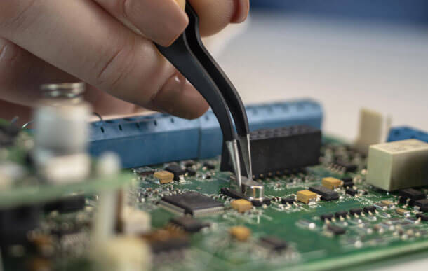
Physical Design
Physical design is a process in the VLSI system in which the structural netlist is transferred from the front-end design to the back-end design team for transforming into a physical layout database that contains geometrical design information for every physical layer and is used for interconnections. Tessolve’s physical implementation services include :
Motivated team, better design capability
- Rich and extensive Physical Design (PD) experience has enabled the team to work on multiple successful tape-outs.
- Expertise with all Industry standard EDA tools, Design Flow and well-trained to handle low power, high-performance area critical designs.
Why Tessolve
At Tessolve, we help individuals realize their full potential, fostering excellence with our wholesome working environment. To our employees, we bring exposure to the latest technology, and an opportunity to explore the application of silicon engineering across a wide breadth of industries. It means, you have the chance to work with globally diverse customers on cutting edge engineering projects while growing with a top tier company that is a pioneer in hardware testing.
Core Values of Tessolve
Representing how we operate every day and grow stronger

People-Centric
We treat our employees with respect and fairness while earning their trust and fostering excellence.

Customer Focused
We focus on creating value for our customers and enable them to bring quality products to market faster and in a cost-effective way.

Engineering Excellence
We take pride in our work and strive for engineering excellence in everything we do. We are always self-driven and proactive.

Entrepreneurial
We think out-of-the-box and innovate. We take challenges as opportunities and use them to enhance our experience and expertise.
Worldwide Career Opportunities
Be part of an extended team of our customers and your work has the potential to shape the machinery that goes into the world’s cutting-edge technology and products.

Customer Turnkey Solutions

End To End Execution

Custom Silicon Qor Recipes

Die Size, TAT, Power, Timing

Deep And Wide Expertise

SoC RTL to GDSII

Execution Experience

Multiple complex SoCs delivered at lower nodes

Flexible deployment at any stage without impacting project schedules

Meet aggressive timelines
Innovation & Technology
If you want to design and build the hardware technologies for world’s largest and most powerful AI computing, wireless technologies, processors, and memories.


