Tessolve’s Chiplet Design Services provides a cutting-edge solution for semiconductor companies looking to push the boundaries of performance and efficiency. By leveraging advanced chiplet architecture, Tessolve enables the integration of multiple specialized components within a single package, optimizing for power, performance, and area. With a focus on customization, we tailor each project to meet specific client needs, fostering innovation and accelerating time-to-market. Trust Tessolve to deliver next-generation chiplet solutions that drive technological advancement and competitive advantage.
Key Objectives
- Enhance Performance and Efficiency
- Customization to Client Needs
- Accelerate Time-to-Market
- Ensure High Quality and Reliability
- Drive Innovation
Enhance Performance and Efficiency
Develop chiplet solutions that significantly boost the performance and efficiency of semiconductor products, leveraging advanced architecture and integration techniques.
Customization to Client Needs
Tailor chiplet designs to meet each client’s specific requirements and goals, ensuring bespoke solutions that address unique challenges and opportunities.
Accelerate Time-to-Market
Streamline the design, development, and validation processes to reduce time-to-market, enabling clients to quickly capitalize on new technological advancements.
Ensure High Quality and Reliability
Implement rigorous testing and validation protocols to ensure that all chiplet designs meet the highest standards of quality and reliability, minimizing the risk of failure in the field.
Drive Innovation
Foster continuous innovation in chiplet design and integration, staying ahead of industry trends and providing clients with cutting-edge solutions.
Chip Design Solutions
Chiplet Design – This design has multiple dies with different locations. Here we have used the UCIE Standard protocol to achieve the connectivity between the dies. We used 32 bits of data lines for connecting multiple dies.
Solution Delivered
- 14 layers substrate
- 6-2-6 buildup
- BGA , 17mmx17mm , 0.8 mm pitch
- Multiple power supplies for different dies
- Controlled impedance for 50E,100E
- Transmission and Receiver lanes
This is a design with 6 Dies placed at different locations with different orientations and length. This design has UCIE Standard technology. North and East bump coordinates had UCIE interface to connect between multiple dies. Multiple netlist were created for different dies to achieve the connectivity. We had maintained 500 microns tolerance of length matching between the signals. We have tried to achieve the maximum length of the signals within UCIE protocol limit. Minimum Length is 2mm and Maximum Length is 25mm.
Chiplet Design Solution
| Sr No. | Packge Design Attribute | Values |
|---|---|---|
| 1 | #dies per package | 10 ->(Chiplet_1 - 6, Chiplet_2 - 4) |
| 2 | Layer Count | 5-2-5 |
| 3 | Package size | 40x40mm |
| 4 | BGA Ball pitch | 1mm |
| 5 | Package build-up Material | GL102 |
| 6 | #Test Sites | Total 5 3-(20mm)-> Long Traces 2-(5mm)-> Short Traces |
| 7 | Speed | 16Gbps |
| Sr No. | Packge Design Attribute | Values |
|---|---|---|
| 1 | #dies per package | 10 (Chiplet_1 - 6, Chiplet_2 - 4) |
| 2 | Die Technology | Chiplet_1 6nm TSMC & Chiplet_2: 12nm TSMC |
| 3 | Die size | Chiplet_1: 1.284mm x 3.264mm (4.2 sqmm) Chiplet_2: 2.5mm x 2.6mm (6.5 sqmm) |
| 4 | Bump pitch | 130um |
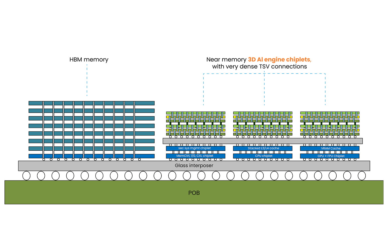
Chiplets Strategies for Large Scale SoCs

The demand for higher-performing and more power-efficient Integrated circuits (ICs) continues.

Large scale SoCs and AI/ML based chips are adopting Chiplet based design techniques.

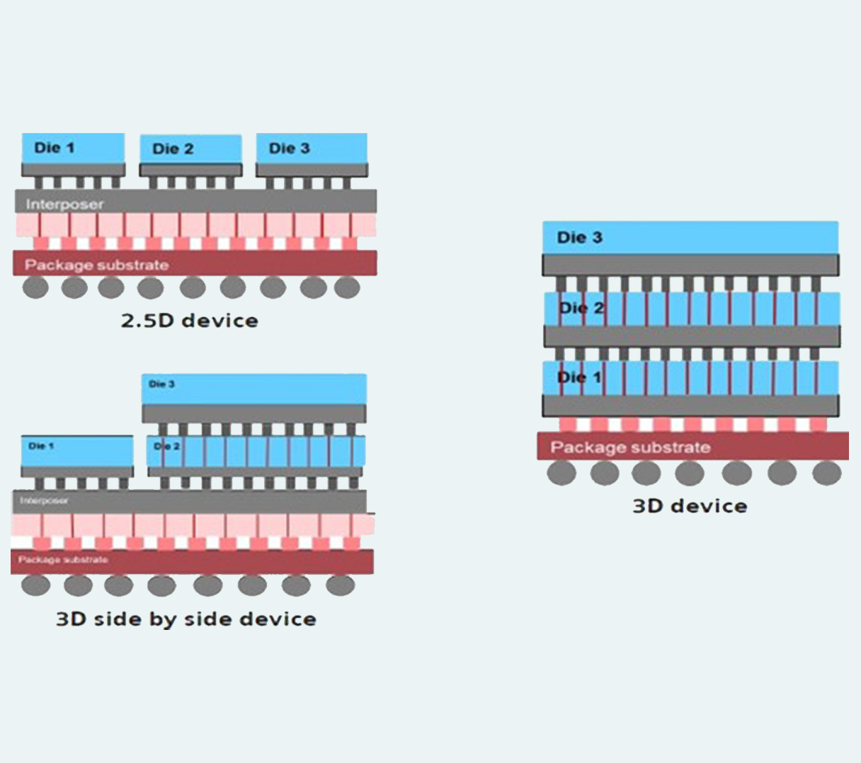
Next-generation devices increasingly feature complex architectures that connect 3D IC (vertical) or 2.5D (side- by-side) dies so that they behave as a true System-in-Package.

AI accelerators need to perform parallel processing or large amounts of data, which would require HBM(High Bandwidth Memory) transactions and high compute capability.
Expertise In A Nutshell
Mastery of diverse signals and ATE platforms
End-to-end semiconductor solution development – from chip design, test, and PCB engineering through post-silicon support.
Faster time-to-market through deep domain expertise in Analog, Digital, Mixed Signal, and RF.
Broad ATE platform experience and built-in infrastructure including a test floor, characterization, reliability lab, and PCB FAB.
The ability for clients to leverage high-end semiconductor engineering in a cost-effective model as we scale teams to meet the exact customer needs.
Expertise To Outcomes
Leading good ideas to great products

EDA Solutions for Multi-Die Chip
- EDA Multi-die tools help customers speed and simplify critical design-for-test (DFT) tasks for next-generation ICs based on 2.5D and 3D architectures.
- Known good die (KGD) testing of bare dies achieved before they go into a multi-die package. The target die could be selected by PTAP/STAP setup.
- The Tessent Streaming Scan Network (SSN) bus can be reused as the Flexible Parallel Port (FPP) as defined by the standard.
- Streaming Fabric is an alternate solution for the FPP(Flexible Parallel Port) interface across chiplets.
Die Tests:
- Interconnect Tests: Using wrapper EXTEST or BScan EXTEST.
- Top die INTEST and MBIST: Feedthrough or Bypass the lower die.
- The base die INTEST and MBIST: Skip the top dies.
- Test setup programming for PTAP / STAPs.
Configuration strategy for Multi-Die Chips – HBM
- Memories could be stacked in an interposer or a separate die for HBM transactions. This could aid high compute capability.
- Multi-die memory BIST and memory repair are supported through TAP and IJTAG.
- IJTAG complements both 2.5D and 3D tests, including serialized scans through PTAP and IJTAG as required by the IEEE 1838 standard.
- TAP/IJTAG can be used with embedded IP core tests.
Configuration strategy for Multi-Die Chips – HSAT
- Streaming Fabric can provide higher test bandwidth with a new technology called SiliconMAX High-Speed Access and Test(HSAT).
- This leverages high-speed functional I/Os(HSIO) such as PCIe or USB to drive scan network.
- The implementation strategies of HSAT for 2.5D and 3D designs are shown in the figures.
Why Tessolve?
Our extensive experience in chip design and integration, coupled with a commitment to cutting-edge technology, ensures that we deliver superior performance and efficiency tailored to your specific requirements. Tessolve’s holistic approach covers every stage of the design process, from initial concept and development to rigorous testing and validation, guaranteeing high-quality, reliable outcomes.
Package Testing with BSCAN Feature Enables
For testing connections between stacked logic die, boundary scan cells are automatically inserted at each through silicon via (TSV) just as they would be for regular IO pads. Boundary scan patterns are then generated to target faults in the TSV interconnect.
- 2.5D and 3D SoC assembly may result in die-to-die interconnect defects.
- Boundary scan interconnect tests are run inside the SoC using advanced algorithms to target multiple defect types.
- Package-level “unified” boundary scan description language (BSDL) files could be generated to incorporate the SoC-level package pins for board and system-level interconnect testing.


