In the dynamic realm of electronics, expeditious PCB design holds paramount importance. These PCB design boards represent the intricate pathways through which electrical impulses traverse within sophisticated devices. Upholding the integrity of these signals at high velocities is imperative for the proper functioning and reliability of electronic systems. In this context, channel modeling and simulation are invaluable tools for PCB design engineers, both domestically and internationally.
What are Channels in High-Speed PCB Design?
The physical routes on a PCB design board that transfer electrical signals between components are called channels. These channels can have different electrical properties, such as regulated impedance traces, microstrip lines, or strip lines. These channels can significantly affect signal integrity in high-speed setups where signal frequencies approach gigahertz (GHz) ranges. Crosstalk, reflections, and signal loss are examples of factors that might distort the signal and cause problems with performance or even total system failure.
Get in touch
The Challenge of High-Speed Signals
The traditional methods of PCB design are no longer sufficient as data transfer rates on PCB hardware rise, often surpassing the gigahertz range. Ensuring signal integrity with simple rules of thumb is no longer possible. Several types of impairments can affect high-speed signals, including:
- Crosstalk: Unwanted coupling of electrical energy between adjacent traces, causing signal distortion.
- Reflections: Impedance mismatches in the transmission line cause reflections, which deteriorate the signal by bouncing it back.
- Signal Loss: Signal loss is the weakening of a signal caused by dielectric losses and conductor resistance as it moves along the trace.
Bit errors, decreased data speed, and even system failure can result from these impairments.
The Role of Channel Modeling
The process of mathematically representing the electrical behavior of a PCB design board is referred to as channel modeling. This modeling technique translates the physical characteristics of the trace, such as width, thickness, and dielectric properties, into equations that define the signal propagation across the channel.

Two main types of channel models are utilized in high-speed PCB design:
- S-parameter Model: Scattering parameter models, or S-parameter models, describe the transmission line as a whole, including the connections via holes and traces. They provide information on how much of the signal is reflected, transmitted, and lost at various frequencies, representing the channel’s behavior in the frequency domain.
- IBIS Models (Input/output Buffer Information Specification): These models concentrate on how the integrated circuit (IC) pins on the printed circuit board (PCB) drive and receive signals. They offer details on the parameters of the driver’s output voltage and current as well as the input impedance and sensitivity of the receiver.
Types of Channel Modeling for High-Speed PCBs

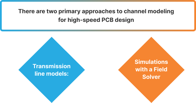
There are two primary approaches to channel modeling for high-speed PCB design:
- Transmission line models: These models show the channel as a collection of grouped components, such as inductors, capacitors, and resistors. Although they are very easy to construct, they might not be accurate for high-frequency applications or complex channels.
- Simulations with a Field Solver: These simulations use advanced software to solve Maxwell’s equations and extract the channel’s entire electromagnetic activity. Although this approach yields the most precise results, it can be costly and time-consuming in terms of computing.
Simulation and Analysis
A channel model can be utilized for simulation after it has been developed. Engineers can forecast how the real signal will behave on the actual PCB design board in the USA by feeding a test signal into the model and examining the result. PCB design engineers have access to several simulation tools, such as:
- Frequency-domain simulation: Through the analysis of the channel’s frequency response, frequency-domain modeling offers insights into phase shift and signal attenuation at various frequencies.
- Time-domain simulation: This method replicates the real-time waveforms of voltage and current on the transmission line. It enables the visualization of problems with signal integrity, such as reflections and crosstalk.
Benefits of Channel Modeling and Simulation
Modeling the channel behavior before manufacture can help detect and resolve signal integrity concerns early, saving time and money.
- PCB layout optimization: By modifying trace lengths and spacing to reduce crosstalk, for example, the layout of the PCB design board can be made more efficient with the help of simulation.
- Enhanced design confidence: Before spending a lot of money on costly manufacturing, PCB design experts can feel more confident in their designs by using simulation to confirm the channel’s performance.
- Reduced time to market: New products’ time to market can be expedited by identifying and fixing signal integrity issues early in the design cycle.
Conclusion
Channel modeling and simulation are indispensable tools for PCB design engineers working on high-speed PCB design boards in the USA and around the world. Engineers can guarantee the signal integrity of their designs and produce dependable and high-performing electronic devices by building precise models and applying simulation techniques. These methods will become increasingly crucial as technology develops, guaranteeing the successful creation of state-of-the-art electronic equipment.


